Logic From Switches (transistors → gates → adder → memory)
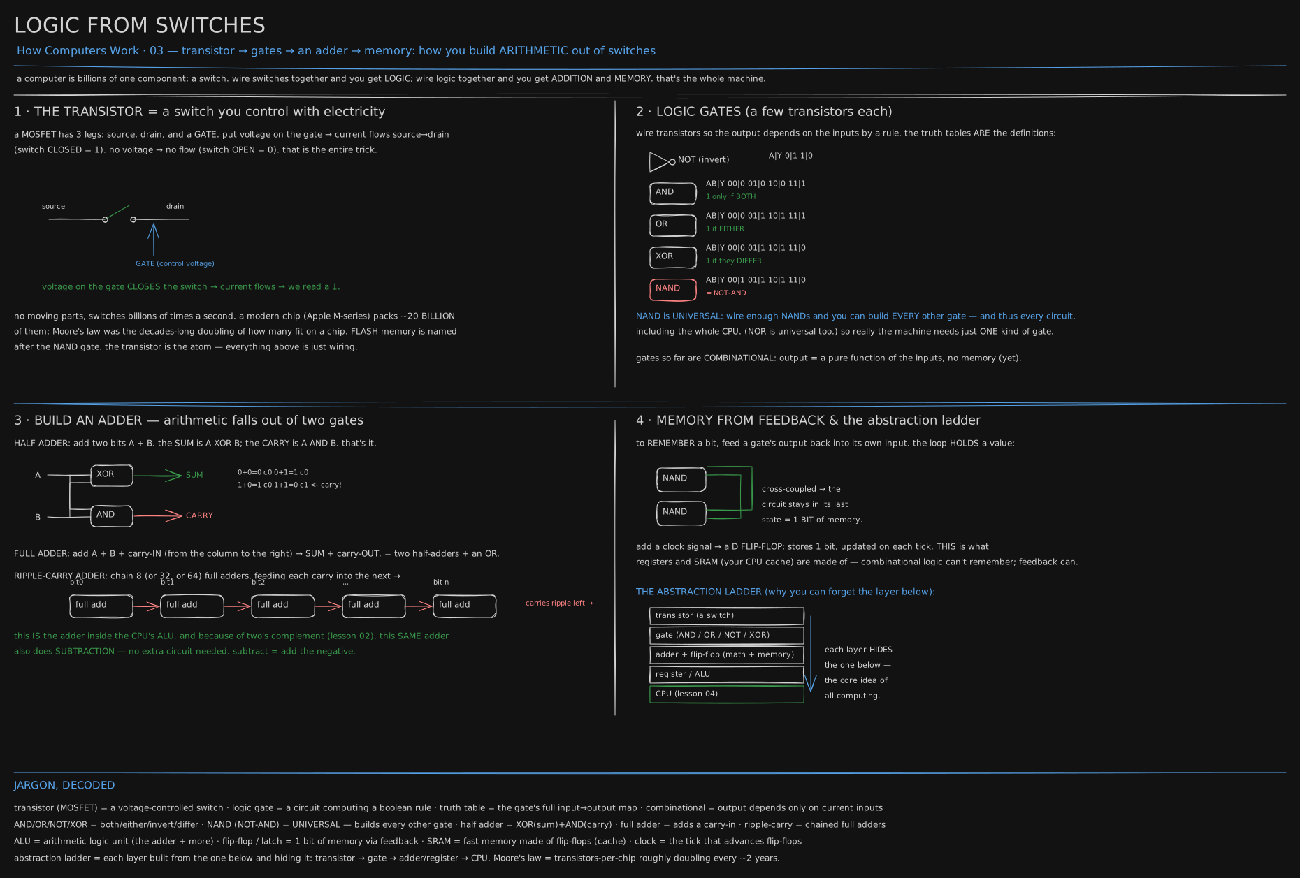
The same wall of switches turning into gates, an adder, and a loop that remembers, walked through here in words instead of a diagram.
Before you start. Everything Is a Number (bits & bytes) showed a computer stores everything as switches wired into bytes, each one only on or off. Numbers for Real (signed ints, overflow, floating point) showed a byte holds just 256 patterns, so a sum needing a 257th loses its top bit. This lesson is where those switches start doing work: adding numbers, and holding onto the answer after the switches that made it have moved on.
1936: the machine at MIT nobody could redesign without weeks of guessing
At MIT there was a room-sized machine called the differential analyzer, built by professor Vannevar Bush: gears and disks that solved calculus problems by physically turning. Wiring it for a new problem meant rewiring a tangle of control relays, with no theory to guide it - an engineer tried something, and if the machine misbehaved, tried again.
A 20-year-old graduate student named Claude Shannon ran the machine in 1936. As an undergraduate at the University of Michigan he had studied a Victorian-era oddity: George Boole’s algebra of “true” and “false”, with no known use outside philosophy. Watching the relays in Bush’s machine, Shannon noticed that a relay is only ever open or closed - exactly the two values Boole’s algebra worked with.
In 1937 he wrote it up as his master’s thesis, A Symbolic Analysis of Relay and Switching Circuits: any switching circuit could now be designed on paper with Boole’s rules instead of guessed at by hand. His thesis even included a circuit that adds binary numbers - the same thing you’re about to build, ninety years later.
Today’s switch: no moving parts, and no finger required
A light switch on your wall is a switch: flip it, current flows or it doesn’t. Shannon’s engineers used a relay - a switch flipped by an electromagnet instead of a hand, letting one circuit trigger another automatically. The switch inside your phone is smaller still: a transistor, with no moving parts. Voltage on its control leg lets current through; take the voltage away and it stops. That’s the whole trick, flipping billions of times a second - a modern chip packs about 20 billion of them.
The shape carries over from Shannon’s relays exactly: on, or off. Only the speed and the size changed.
Gates: wiring switches to answer one question
Wire a handful of switches so the output follows one fixed rule about the inputs, and you get a gate: AND lights up only when both inputs are on, OR when either is, NOT flips whatever it’s given. The clearest way to show a gate is a table of every input and its answer; read 01|0 as inputs 0 and 1, output 0:
NOT   A|Y  0|1  1|0                 (invert)
AND   AB|Y 00|0 01|0 10|0 11|1      (1 only if BOTH)
OR    AB|Y 00|0 01|1 10|1 11|1      (1 if EITHER)
XOR   AB|Y 00|0 01|1 10|1 11|0      (1 if they DIFFER)
NAND  AB|Y 00|1 01|1 10|1 11|0      (NOT-AND)
One row is worth sitting with: NAND, “NOT of AND”, answers 1 in three cases out of four. It sounds impossible that wiring enough of just that gate could rebuild every other rule, but it works: NOT is a NAND fed the same signal twice, AND is a NAND then a NOT, and OR follows. Wire enough NANDs and you can build any circuit at all, including the chip you’re reading this on. Every gate so far only looks at its inputs right now - none remember anything yet.
Two gates add a bit, and a third is where addition gets interesting
Add two single bits, A and B. The sum is 1 when A and B differ - what an XOR gate already answers. The carry, the bit spilling into the next column, is 1 only when both are on - what an AND gate already answers. Two gates, wired side by side, are a complete adder for one bit:
1 + 1 = 0 carry 1 (that's why 1+1 needs a carry bit)That row is the whole reason a carry exists: one plus one is two, and two needs a second column to write, 10 in binary.
Real addition needs a third input too - a carry arriving from the column to its right - so a full adder is two one-bit adders plus one gate to combine their carries. Chain eight of them, each carry feeding the next, and you can add two whole bytes:
flowchart LR
  subgraph column0["bit 0"]
    A0["a0, b0"] --> F0["full adder 0"]
  end
  subgraph column1["bit 1"]
    A1["a1, b1"] --> F1["full adder 1"]
  end
  subgraph column2["bit 2"]
    A2["a2, b2"] --> F2["full adder 2"]
  end
  C0["carry in: 0"] --> F0
  F0 -->|carry| F1
  F1 -->|carry| F2
  F2 -->|carry| C3["carry out, to bit 3 ... bit 7"]
  F0 --> S0["sum bit 0"]
  F1 --> S1["sum bit 1"]
  F2 --> S2["sum bit 2"]
Follow only the carry arrows: every column depends on the carry limping in from the one before it. That dependency is what makes a wide adder real engineering, not “wire it eight times” - the last bit can’t be trusted until every earlier carry has settled, and how long that takes limits how fast the clock can tick, worked out on paper in the second half.
Memory from feedback: the loop that remembers
Every gate so far forgets the instant its inputs change - no wire stores a fact. But wire two NAND gates so each one’s output feeds the other’s input, and the loop does something no single gate can: it holds its state, even after you stop asking it to.
This pair is called a latch, and the easiest way to see it is as one circuit with two buttons and two resting states:
stateDiagram-v2
  [*] --> Holding0
  Holding0 --> Holding1: press S (set)
  Holding1 --> Holding0: press R (reset)
  Holding0 --> Holding0: nothing pressed, output stays 0
  Holding1 --> Holding1: nothing pressed, output stays 1
With neither button pressed, the loop keeps whatever it last had - that’s the memory. Add a clock wire so it can only change its mind once per tick, and you get a flip-flop: the same loop, timed. A row of these, each holding one bit, is what your CPU calls a register - the next lesson runs on exactly that.
You now know
- A transistor is a switch flipped by electricity instead of a hand; a modern chip packs about 20 billion of them.
- Wire switches to answer one fixed yes/no rule and you get a gate; one kind, NAND (off only when both inputs are on), can build every other gate there is.
- Two gates - one answering “do they differ”, one “are both on” - add a single bit and its carry; chain eight and you can add a whole byte.
- A carry ripples through every column in order, one at a time, and that ripple is what limits how fast an adder - and the chip around it - can run.
- Feed a gate’s output back into itself and the loop holds a value after the inputs that set it are gone - that loop is a latch, where memory begins.
- A clocked latch is a flip-flop, and a row of them is a register - the CPU’s own memory, one lesson from now.
Stop here if you want. What follows is the same circuit run in code, with the gate counts and the clock speed they buy.
Second read: the adder, built from one gate and run
“NAND is universal” and “two gates make an adder” are claims you can settle in a script instead of taking on faith. The listing below defines one primitive, NAND; nothing else touches a & or | after that line, and every other gate, the half adder, the full adder, and an 8-bit adder are wired from it, the way a chip would.
// every gate from one primitive: NAND
const NAND = (a, b) => 1 - (a & b);
const NOT  = a => NAND(a, a);
const AND  = (a, b) => NOT(NAND(a, b));
const OR   = (a, b) => NAND(NOT(a), NOT(b));
const XOR  = (a, b) => { const n = NAND(a, b); return NAND(NAND(a, n), NAND(b, n)); };
// half adder: two bits in, sum and carry out
const half = (a, b) => ({ sum: XOR(a, b), carry: AND(a, b) });
// full adder: three bits in (a, b, carry-in), two half adders and an OR
const full = (a, b, cin) => { const h1 = half(a, b), h2 = half(h1.sum, cin); return { sum: h2.sum, carry: OR(h1.carry, h2.carry) }; };
console.log("half adder      a b | sum carry");
for (const a of [0, 1]) for (const b of [0, 1]) { const r = half(a, b); console.log(`                ${a} ${b} |  ${r.sum}    ${r.carry}`); }
console.log("\nfull adder    a b cin | sum cout");
for (const a of [0, 1]) for (const b of [0, 1]) for (const c of [0, 1]) { const r = full(a, b, c); console.log(`              ${a} ${b}  ${c}  |  ${r.sum}   ${r.carry}`); }
// ripple-carry: 8 full adders in a chain = the board's 8-bit adder
const bits = n => [...Array(8)].map((_, i) => (n >> i) & 1);            // least significant first
function add8(x, y) { let c = 0; const out = []; for (let i = 0; i < 8; i++) { const r = full(bits(x)[i], bits(y)[i], c); out.push(r.sum); c = r.carry; } return { value: out.reduce((acc, bit, i) => acc + bit * 2 ** i, 0), carryOut: c }; }
for (const [x, y] of [[65, 3], [200, 100], [255, 1], [127, 1]]) { const r = add8(x, y); console.log(`${x} + ${y} = ${r.value}  carry out ${r.carryOut}${r.carryOut ? "  (overflow: the 9th bit fell off)" : ""}`); }
// how many NAND gates did that take?
let count = 0; const N = (a, b) => { count++; return 1 - (a & b); };
const NOT2 = a => N(a, a), AND2 = (a, b) => NOT2(N(a, b)), OR2 = (a, b) => N(NOT2(a), NOT2(b)), XOR2 = (a, b) => { const n = N(a, b); return N(N(a, n), N(b, n)); };
const full2 = (a, b, cin) => { const s1 = XOR2(a, b), c1 = AND2(a, b), s2 = XOR2(s1, cin), c2 = AND2(s1, cin); return { sum: s2, carry: OR2(c1, c2) }; };
full2(1, 1, 1); console.log(`\none full adder = ${count} NAND gates, so an 8-bit adder = ${count * 8}, a 64-bit adder = ${count * 64}`);
half adder a b | sum carry
0 0 | 0 0
0 1 | 1 0
1 0 | 1 0
1 1 | 0 1
full adder a b cin | sum cout
0 0 0 | 0 0
0 0 1 | 1 0
0 1 0 | 1 0
0 1 1 | 0 1
1 0 0 | 1 0
1 0 1 | 0 1
1 1 0 | 0 1
1 1 1 | 1 1
65 + 3 = 68 carry out 0
200 + 100 = 44 carry out 1 (overflow: the 9th bit fell off)
255 + 1 = 0 carry out 1 (overflow: the 9th bit fell off)
127 + 1 = 128 carry out 0
one full adder = 15 NAND gates, so an 8-bit adder = 120, a 64-bit adder = 960Read it in four parts. The half adder table is generated, not typed in: XOR gave the sum column, AND gave the carry column, and 1 1 | 0 1 is the whole reason a carry exists. The full adder table has a row the half adder can’t reach: 1 1 1 gives sum 1, carry 1, three in binary - and one OR is enough to combine the two carries, because the first half adder only carries when a and b are both 1, and then its own sum is 0, so the second can never carry too. Eight in a chain add real bytes, edges included: 65 + 3 = 68 is ordinary, but 200 + 100 should be 300, nine bits long, and the chain reports 44 with carry-out set - the ninth bit fell off, 300 mod 256 = 44, the same wraparound the previous lesson counted, kept in the CPU’s carry flag so software can notice. 127 + 1 = 128 carries out 0, correct unsigned; only the signed reading calls 1000 0000 minus 128, and the adder doesn’t know which you meant. Because of two’s complement, this same adder does subtraction too: flip B’s bits and start the chain with a carry-in of 1, and it becomes a subtractor, no new circuitry needed. Last, the gate count is the price of the abstraction: 15 NANDs per full adder here (the textbook minimum is 9), 120 for a byte, 960 for a 64-bit adder.
That gate count sets a real speed limit. A CMOS NAND switches in about 20 picoseconds on a modern process, and a carry crosses roughly two gate delays per column:
 64 columns × 2 gates × 20 ps  =  2,560 ps  ≈  2.6 ns   →  one add per 2.6 ns  =  ~390 MHz ceiling  ✗
 lookahead, log₂(64) = 6 levels × 2 gates × 20 ps  =  240 ps  →  ~4 GHz                            ✓
The chip you’re reading this on runs at 3-4 GHz, so it can’t be rippling 64 bits straight through: carry-lookahead, computing several carries at once instead of waiting for each, isn’t an optimisation here - it’s the only way the clock gets there. The transistor cost is small by comparison: 15 NANDs × 4 transistors is 60 per full adder, 3,840 for a 64-bit adder, against 20 billion on the die, 0.00002%. The adder isn’t where the transistors go; the caches and the machinery for running many instructions at once are, and The Memory Hierarchy (cache, locality, the memory wall) counts them.
The whole ladder, in one look:
transistor (a switch)
  → gate (AND/OR/NOT/XOR)
    → adder + flip-flop (math + memory)
      → register / ALU
        → CPU  (lesson 04)
Each layer is built from the one below it and hides it: you can design a CPU thinking in registers without tracking a single transistor, the same trick that lets a socket hide TCP hide IP hide frames, all the way down.
Try it
Play nandgame.com or work through Nand2Tetris Project 1–2: build a NOT, AND, XOR, half-adder and full-adder from a single NAND, then wire an ALU. An hour there makes this board permanent. Or in code, implement xor/and from nand only and build a full_adder(a,b,cin) - watch arithmetic appear from one gate.
The listing above is that exercise done; save it as gates.mjs and run it:
node gates.mjsThen break it, three ways, one line each:
- Change
XORto returnOR(a, b)and re-run. The half adder table now says 1 + 1 = 1 carry 1, three, and every sum in the byte tests is wrong. The difference between “either” and “differ” is the difference between arithmetic and nonsense. - Widen the chain: change the
8inbitsandadd8to16, add[65535, 1]to the test pairs.200 + 100is now 300 with no carry-out,255 + 1is 256, and only65535 + 1wraps to 0 - the ninth bit no longer falls off, the seventeenth does (the message string still says “9th”; fix that too). - Count the gates on a 64-bit ripple adder’s longest path: 64 full adders, and in each the carry crosses an AND and an OR, so at least 64 x 2 gate delays before the top bit is right. At a few tens of picoseconds per gate that’s several nanoseconds, longer than a 4 GHz clock’s 0.25 ns tick - why no real chip ripples 64 bits.
Down to the bytes
Gate-level companion: Full Adder Gate Diagram - the half adder (XOR=sum, AND=carry), the full adder (two halves + OR), and four of them chained to compute 0101 + 0011 = 1000 (5+3=8) with the carry rippling right-to-left.
Go deeper
- The Elements of Computing Systems (Nand2Tetris) - Nisan & Schocken (build a computer from a NAND up)
- Ben Eater - building an 8-bit computer on breadboards (watch a real ALU get wired)
- Code - Petzold (chapters on relays, gates, and adders)
- nandgame.com.
Related
- The CPU (fetch-decode-execute, the ISA, assembly) is next: the clock this lesson put a ceiling on, and the registers built from its flip-flops.
- The Memory Hierarchy (cache, locality, the memory wall) takes those registers on to caches and RAM.
- The full How Computers Work list is in CURRICULUM.
Retrieval practice
9 questions. Answer each one before you open it.
How is a transistor a “switch,” and what makes it different from a light switch or a relay?
A transistor conducts current through its control leg only when voltage is applied - a switch whose state is set by another electrical signal, not a hand or an electromagnet. That’s what lets switches control other switches automatically, with no moving parts, flipping billions of times a second.
What does it mean that NAND is “universal”?
Any boolean rule - hence any digital circuit, up to a whole CPU - can be built from NAND gates alone: NOT is a NAND with tied inputs, AND is a NAND then a NOT, and so on. A manufacturer could build everything from one gate type. NOR shares this property.
Give the two gates of a half adder and what each output is.
Sum = A XOR B (1 when the bits differ), carry = A AND B (1 only when both are 1, i.e. 1+1). A full adder also takes a carry-in, so full adders chain (ripple-carry) to add wide numbers.
Why can the same adder circuit do subtraction?
Because signed numbers use two’s complement, where subtracting B is the same as adding B’s two’s-complement. Flipping B’s bits and starting the chain with a carry-in of 1 turns the existing adder into a subtractor - no separate circuit is needed.
Why can’t a gate remember a bit, and what fixes it?
A gate’s output is purely a function of its present inputs, so nothing holds a value once the inputs move on. Feeding an output back into the input creates a stable feedback loop, a latch, that keeps its state until deliberately changed. Registers and cache memory are arrays of these loops, clocked.
What is the ladder from transistor to CPU, and why does it matter?
Transistor to gate to adder-and-flip-flop to register/ALU to CPU: each level is built from the one below and hides its complexity. It matters because you can reason at one level without tracking billions of transistors - the same principle that lets a socket hide TCP without you thinking about electrons.
In the full adder, why is a single OR enough to combine the two half adders’ carries?
The first half adder carries only when a and b are both 1, and then its sum is 0, so the second, adding that sum to the carry-in, can’t carry too. The two carries are never 1 together, so OR gives the right answer in every row, including 1+1+1 = sum 1, carry 1.
Add 200 + 100 on an 8-bit ripple-carry adder. What comes out, and where did the rest go?
44, with the carry-out bit set. 300 is nine bits long (1 0010 1100), and the top bit falls off the eighth adder; 300 mod 256 = 44. The carry-out is the same lost carry as the previous lesson’s wrap-around, kept in the CPU’s carry flag so software can detect the overflow.
Why does the length of the carry path, not the number of gates, set how fast the adder can run?
Every column’s carry-in depends on the one before it, so the last bit can’t settle until all the earlier carries have, even though data enters every column at once. That longest chain of gate delays is the critical path, and the clock can’t tick faster than it; carry-lookahead adders spend extra gates to shorten it.